
During the PCB Assembly processing and PCB soldering process, the performance of the flux directly affects the quality of the solder. So what are the common soldering defects in PCBA processing? How to analyze and improve the bad soldering that occurs?
- Bad condition: There are too many residues on the PCB surface after welding, and the board is dirty.
Result analysis:
(1) The temperature is not preheated before welding or the preheating temperature is too low, and the temperature of the tin furnace is not enough;
(2) The speed of the board is too fast;
(3) Anti-oxidant and anti-oxidation oil are added to the tin liquid;
(4) too much flux coating;
(5) The component feet and the orifice plate are not proportional (the holes are too large), so that the flux is accumulated;
(6) During the use of the flux, no diluent is added for a long time.
- Bad condition: easy to catch fire
Result analysis:
(1) There is no air knife in the wave furnace itself, causing the flux to accumulate and dripping onto the heating tube during heating;
(2) The angle of the air knife is incorrect (the flux distribution is uneven);
(3) There is too much glue on the PCB, and the glue is ignited;
(4) The running speed is too fast (the flux is not completely volatilized, dripping into the heating tube) or too slow (the board surface is too hot);
(5) Process problems (PCB plate, or PCB is too close to the heating tube).
- Bad condition: Corrosion ( green component, black solder joint)
Result analysis:
(1) Insufficient preheating causes too much flux residue and too much residue;
(2) Use the flux that needs to be cleaned, but it is not cleaned after the soldering is completed.
- Bad condition: connected to electricity and leakage (insulation is not good)
Result analysis:
(1) The design of PCB is unreasonable
(2) PCB solder mask is of poor quality and easy to conduct
- Bad phenomenon: virtual solder, continuous solder, leakage solder
Result analysis:
(1) The amount of flux coating is too small or uneven;
(2) Some of the pads or solder fillets are heavily oxidized;
(3) The PCB layout is unreasonable;
(4) The foaming tube is clogged, the foaming is uneven, and the flux coating is uneven;
(5) Improper operation method when hand immersion tin;
(6) The inclination of the chain is unreasonable;
(7) The wave is not flat.
- Bad phenomenon: the solder joint is too bright or the solder joint is not bright
Result analysis:
(1) This problem can be solved by selecting a bright or matte type flux;
(2) The solder tin used is not good.
- Bad phenomenon: smoke is big and tastes great
Result analysis:
(1) The problem of the flux itself: the use of ordinary resin is relatively large; the activator smoke is large and has a pungent odor;
(2) The exhaust system is not perfect.
- Bad phenomenon: splash, solder ball
Result analysis:
(1) Process: preheating temperature is low (the flux solvent is not completely volatilized); the plate speed is fast, the preheating effect is not reached; the chain inclination angle is not good, there is a bubble between the tin liquid and the PCB, and the solder ball are generated after the bubble bursts; Improper operation when immersed in tin; working environment is damp;
(2) The problem of PCB: the board surface is damp, there is moisture; the design of the hole of PCB running gas is unreasonable, causing the air between PCB and tin liquid; the design of PCB is unreasonable, and the feet of the parts are too dense to cause the gas.
- Bad phenomenon: the tin is not good, the solder joint is not full
Result analysis:
(1) The double waving peak process is used, and the active component of the flux is completely volatilized when the tin is passed once;
(2) The running speed is too slow and the preheating temperature is too high;
(3) uneven coating of flux;
(4) The pads and component pins are severely oxidized, resulting in poor tin consumption;
(5) The flux coating is too small to completely wet the pads and component leads;
(6) The design of pcb is unreasonable, affecting the tinning of some components.
- Bad phenomenon: PCB solder mask peeling off, peeling or foaming
Result analysis:
(1) More than 80% of the reasons are problems in the manufacturing process of PCB: poor cleaning, inferior solder mask, PCB board and solder mask mismatch;
(2) The temperature of the tin liquid or the preheating temperature is too high;
(3) too many solder times;
(4) When the hand is immersed in tin, the PCB stays on the surface of the tin liquid for too long.
The above is the analysis of poor soldering phenomena and results in the processing of PCBA.
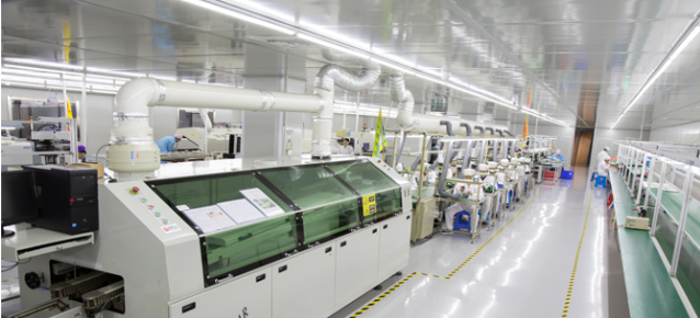
RауMing Tесhnоlоgу is a wоrld-lеаding PCB Manufacturing аnd Aѕѕеmblу company оffеring dоublе-ѕidеd аand multilауеr рrintеd сirсuit boards manufacturing services. Have 10 years PCB soldering experience ,If you want to know more about PCB soldering knowledge ,visit www.raypcb.com


